
Designing With Light: How Microchips Are Made Using Photolithography
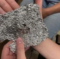 Students design a simple opaque mask using materials such as foilCopyright Doug Picard
Students simulate the photolithography process used in semiconductor manufacturing by using gel nail polish as a UV-sensitive photoresist. They design a simple opaque mask using materials such as construction paper or foil, then place it over the coated disc. Using an overhead UV light, they expose the disc for varying times to simulate under-, proper-, and over-exposure. Uncured gel is removed with acetone, revealing a hardened pattern that mimics how microchips are fabricated. Students analyze the results, compare them to their original mask design, and discuss the effects of exposure time and resolution. This activity connects to NGSS standards in physical science and engineering design by exploring light–matter interactions, energy transfer, and real-world applications in microfabrication.
A semiconductor process engineer designs and optimizes the manufacturing steps for microchips, including photolithography, etching, and deposition. They work closely with materials, chemical, and electrical engineers to troubleshoot issues, improve yield, and implement new technologies. Their efforts ensure that the tiny, high-performance components in computers, smartphones, and other electronics are reliably produced.
After this activity, students should be able to:
- Model the photolithography process by creating a patterned coating on a glass disc using UV-cured gel nail polish.
- Analyze how exposure time and masking affect polymerization and pattern resolution.
- Connect the experiment to real-world applications in semiconductor manufacturing and electronics engineering.
- STEL-1R Develop a plan that incorporates knowledge from science, mathematics, and other disciplines to design or improve a technological product or system.
Grades 9-12
Do you agree with this alignment? - STEL-2T Demonstrate the use of conceptual, graphical, virtual, mathematical, and physical modeling to identify conflicting considerations before the entire system is developed and to aid in design decision making.
Grades 9-12
Do you agree with this alignment? - STEL-7CC Apply a broad range of design skills to their design process.
Grades 9-12
Do you agree with this alignment?
- HS-ETS1-2 Design a solution to a complex real-world problem by breaking it down into smaller, more manageable problems that can be solved through engineering.
Grades 9-12
This resource focuses on the following Three Dimensional Learning aspects of NGSS:
Science & Engineering Practices- Design a solution to a complex real-world problem, based on scientific knowledge, student-generated sources of evidence, prioritized criteria, and tradeoff considerations.Do you agree with this alignment?
Disciplinary Core Ideas- Criteria may need to be broken down into simpler ones that can be approached systematically, and decisions about the priority of certain criteria over others (trade-offs) may be needed.Do you agree with this alignment?
Do you agree with this alignment? - Design a solution to a complex real-world problem, based on scientific knowledge, student-generated sources of evidence, prioritized criteria, and tradeoff considerations.
- HS-ETS1-3 Evaluate a solution to a complex real-world problem based on prioritized criteria and trade-offs that account for a range of constraints, including cost, safety, reliability, and aesthetics, as well as possible social, cultural, and environmental impacts.
Grades 9-12
This resource focuses on the following Three Dimensional Learning aspects of NGSS:
Science & Engineering Practices- Evaluate a solution to a complex real-world problem, based on scientific knowledge, student-generated sources of evidence, prioritized criteria, and tradeoff considerations.Do you agree with this alignment?
Disciplinary Core Ideas- When evaluating solutions it is important to take into account a range of constraints including cost, safety, reliability and aesthetics and to consider social, cultural and environmental impacts.Do you agree with this alignment?
Crosscutting Concepts- New technologies can have deep impacts on society and the environment, including some that were not anticipated. Analysis of costs and benefits is a critical aspect of decisions about technology.Do you agree with this alignment?
Do you agree with this alignment? - Evaluate a solution to a complex real-world problem, based on scientific knowledge, student-generated sources of evidence, prioritized criteria, and tradeoff considerations.
- HS-PS4-1 Use mathematical representations to support a claim regarding relationships among the frequency, wavelength, and speed of waves traveling in various media.
Grades 9-12
This resource focuses on the following Three Dimensional Learning aspects of NGSS:
Science & Engineering Practices- Use mathematical representations of phenomena or design solutions to describe and/or support claims and/or explanations.Do you agree with this alignment?
Disciplinary Core Ideas- The wavelength and frequency of a wave are related to one another by the speed of travel of the wave, which depends on the type of wave and the medium through which it is passing.Do you agree with this alignment?
Crosscutting Concepts- Empirical evidence is required to differentiate between cause and correlation and make claims about specific causes and effects.Do you agree with this alignment?
Do you agree with this alignment? - Use mathematical representations of phenomena or design solutions to describe and/or support claims and/or explanations.
- HS-PS4-5 Communicate technical information about how some technological devices use the principles of wave behavior and wave interactions with matter to transmit and capture information and energy.
Grades 9-12
This resource focuses on the following Three Dimensional Learning aspects of NGSS:
Science & Engineering Practices- Communicate technical information or ideas (e.g. about phenomena and/or the process of development and the design and performance of a proposed process or system) in multiple formats (including orally, graphically, textually, and mathematically).Do you agree with this alignment?
Disciplinary Core Ideas- Solar cells are human-made devices that likewise capture the sun's energy and produce electrical energy.Do you agree with this alignment?
- Information can be digitized (e.g., a picture stored as the values of an array of pixels); in this form, it can be stored reliably in computer memory and sent over long distances as a series of wave pulses.Do you agree with this alignment?
- Photoelectric materials emit electrons when they absorb light of a high-enough frequency.Do you agree with this alignment?
- Multiple technologies based on the understanding of waves and their interactions with matter are part of everyday experiences in the modern world (e.g., medical imaging, communications, scanners) and in scientific research. They are essential tools for producing, transmitting, and capturing signals and for storing and interpreting the information contained in them.Do you agree with this alignment?
Crosscutting Concepts- Systems can be designed to cause a desired effect.Do you agree with this alignment?
- Modern civilization depends on major technological systems.Do you agree with this alignment?
- Science and engineering complement each other in the cycle known as research and development (R&D).Do you agree with this alignment?
Do you agree with this alignment? - Communicate technical information or ideas (e.g. about phenomena and/or the process of development and the design and performance of a proposed process or system) in multiple formats (including orally, graphically, textually, and mathematically).
Each group needs:
- 1 bottle of clear gel nail polish (https://a.co/d/acHQDHA)
- 1 borosilicate glass disc (https://a.co/d/071M3Ph)
- cotton swabs or lens wipes
- 1 sponge, foam brush, or soft applicator.
- mask material (see below)
- nitrile gloves (https://a.co/d/e6Sx2OZ) (1 per student)
- water (for final rinse)
- timer or stopwatch
- small tray or petri dish for developing
- (optional) lint-free cloth (to clean glass disc)
For the entire class to share:
- 1 UV light with overhead mount https://a.co/d/0M4irCG
- 1 bottle of acetone https://a.co/d/6Yd1x1Z
- 1 bottle of isopropyl alcohol
- construction paper, foil, printed transparency (locally sourced)
- access to tap water
- lab wipes/paper towels/sponges (to clean up spills)
- (optional) non-motorized turntable (https://a.co/d/94Nf9x9) (to evenly spread the gel nail polish on the glass disc)
- (optional) hot plate
- (optional) microscope
Students will benefit from the following prerequisite knowledge:
- Basic understanding of the electromagnetic spectrum, particularly UV light and its interactions with matter.
- Familiarity with phase changes or chemical reactions, such as curing or polymerization.
- Introductory lab safety and handling of solvents, including acetone, methanol, and isopropyl alcohol.
- Optional but helpful for context: Awareness of how patterns are used in technology, such as circuits or microchips.
(Stand at the front of the room with a glass disc, UV lamp, and gel nail polish in view. Hold up the disc.)
Today we’re diving into a real-world process that’s at the heart of nearly every electronic device you own: your phone, your computer, even your car. It’s called photolithography, and it’s how engineers put incredibly small patterns—sometimes smaller than a piece of dust—onto materials to make circuits and chips.
(Hold up a phone or gesture to a projector slide showing a microchip.) Have you ever wondered how all of this stuff, like your phone, gets so small and powerful? That level of precision doesn't happen by accident. It happens through a process that combines chemistry, light, and clever design.
(Cue Samsung’s semiconductor manufacturing process video, https://youtu.be/Bu52CE55BN0?si=NHIKV9tT87m02ZlO; 7:43 minutes) Let’s watch this video.
Now, we’re not working in a cleanroom or a billion-dollar semiconductor fab, but we are going to simulate the key steps using glass discs and gel nail polish.
Think about nail polish for a second. Have you or someone you know ever used gel polish that hardens under a UV light? (Pause for responses.)
What do you think is happening at the chemical level when that polish ‘cures’ under UV? (Wait for students to suggest ideas about light causing hardening, chemical change, polymerization, etc.)
Now think bigger: What would happen if we blocked some of that light using a mask—like a stencil—and only let certain parts of the polish harden? (Hold up a simple paper mask with cutouts. Invite quick predictions.)
This is your chance to model what engineers actually do when they’re making microchips. We’ll be masking, curing, and developing a pattern, just like in industry. But here’s the fun part: You get to experiment with exposure times and mask designs.
Think about this question as we get started: What variables might change how sharp or accurate our pattern turns out? And even better: How could we improve it?
(Write the following questions on the board for students to return to later.
What does UV light do to the gel polish at the chemical level?
How does the design of the mask affect the final pattern?
What makes one exposure time better than another?)
Background
Photolithography is a key process in semiconductor manufacturing used to create extremely small and precise patterns on materials such as silicon wafers, which are the foundation of modern electronic devices. The process begins by coating the wafer with a thin layer of light-sensitive material called photoresist. This material is specially designed to undergo a chemical change when exposed to light of specific wavelengths, most commonly ultraviolet (UV) light. The chemical change alters the solubility of the photoresist, so that certain areas can later be washed away while other areas remain, creating a pattern that defines where circuits and components will be built. By carefully controlling the intensity, duration, and angle of light exposure, engineers can produce highly detailed features that are only a few nanometers wide, which is far smaller than what can be made with traditional mechanical tools. This precise control of light and chemistry is what allows engineers to manufacture the tiny, intricate circuits that power computers, smartphones, and other electronic devices.
In this activity, gel nail polish serves as a safe, hands-on substitute for photoresist, because it cures, or hardens, when exposed to UV light. A mask placed between the light source and the coated surface blocks some of the light, so only selected areas harden. After exposure, a solvent removes the uncured gel, leaving a pattern that matches the mask design.
This activity connects to key physical science concepts, including wave behavior (how UV light travels and interacts with materials), chemical change (polymerization of the gel), and energy transfer (light energy causing a chemical reaction). It also mirrors real-world engineering practices: Students prototype designs, test outcomes, evaluate results, and iterate to improve their patterns.
Before the Activity
- Gather materials and make copies of the Photolithography Worksheet (PDF) (1 per student).
- Print copies of the Myth/Fact Assessment Sheet (PDF) (1 per student).
- Print copies of the Myth/Fact Assessment Answer Key (PDF) (for the teacher).
- Clearly identify and place acetone and isopropyl alcohol either in a central location or within groups.
- Get familiar with photolithography and the entire semiconductor manufacturing process (https://youtu.be/Bu52CE55BN0?si=NHIKV9tT87m02ZlO).
During the Activity
Part 1: Introduction, Pre-Assessment, and Mask Design (~45 minutes)
- Give each student a Myth/Fact Assessment Sheet (PDF).
- Read the following Teacher Script: “Today we're going to explore how engineers use light to make tiny patterns on materials, just like how circuits are made in phones and computers. Before we jump into our experiment, I want you to take a few minutes to think about what you already know or what you think you know. You'll see a list of 10 statements. For each one, decide if you believe it’s a Myth (false) or a Fact (true). Circle your answer on the Pre-Test side only. Don’t worry if you’re unsure. This is not graded—it’s just to help us think before we do the activity. You’ll come back to it afterward to see how your thinking has changed.”
- Allow 5-10 minutes for students to complete the chart.
- Do not correct answers yet; this is about personal reasoning and reflection.
- Circulate and observe which statements cause hesitation, which can guide discussion later.
- When everyone finishes the list, have a few volunteers share statements that perhaps surprised them or felt tricky.
- Collect the Myth/Fact Assessment Sheet (PDF) for later.
- Divide class into pairs.
- Give each student a Photolithography Worksheet (PDF).
- Present the problem statement: How can we create the sharpest, most accurate pattern on a glass disc using photolithography techniques adapted for a classroom?
- Present the group objective: Simulate the photolithography process used in semiconductor manufacturing by using gel nail polish as a photoresist and a UV lamp to develop a masked pattern on a glass disc. For each iteration, you will follow the same basic procedures, outlined in the worksheet.
- Describe the success criteria:
- Pattern edges are sharp.
- Mask image matches final result.
- Unintended exposure is minimal.
- Once students understand their objective and goal, give each group time to do Step 1: Brainstorm, Plan and Design.
- Ensure each group brainstorms 2–3 possible mask designs.
- Remind students to choose their group mask design based on the following criteria:
- Level of detail (too fine may blur)
- Contrast between exposed/unexposed regions
- Ease of cutting
- Once each team sketches their chosen design, ask them to predict how UV light might interact with their design, recording their predictions in their worksheets.
- When students are ready to create their mask, make sure they cut their mask materials (e.g., construction paper or foil) to be larger than the glass disc.
- Create a pattern and cut it into the material. The pattern can be anything and should fully encompass the area in which the nail polish was applied.
Aluminum foil with pattern cut into it.Copyright Doug Picard
- After each group has their mask cut out, instruct them to move to Step 2: Apply “Photoresist.”
- Remind students to wear gloves.
- Emphasize that the glass disc needs to be cleaned in the order specified in the worksheet.
- Once dry, have students apply a thin, even layer of clear gel nail polish (photoresist) across the glass disc.
- Optional: Have students place their glass disc with clear gel nail polish applied onto turntable and then turn on the turntable to lightly spin such that the clear gel nail polish evenly spreads across the glass.
- Let the painted glass disc sit for 1–2 minutes to allow the nail polish to self-level.
- At the end of Part 1, each group should have prepared their disc and have their masks ready.
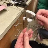 The glass substrate on which the mask is applied.Copyright Doug Picard
Part 2: UV Exposure, Development, Analysis, and Post-Assessment (~45 minutes)
- Instruct students to begin Step 3: Mask and UV Exposure.
- Have students place their opaque mask over the coated glass disc.
- Remind students to keep their mask as flat and close to the glass surface as possible for the best results.
- Note: Students may need to be creative with spacers. Spacers are small objects that create a tiny, controlled gap between the mask and the glass disc. They prevent the mask from touching the photoresist (which could smear the pattern) while keeping it close enough for the UV light to produce a sharp image. Students can solve this engineering sub-problem in a few ways:
- Use small pieces of clean plastic, tape, or foam at the corners of the mask to lift it slightly above the glass.
- Stack thin sheets of paper or cardstock under the edges of the mask for uniform spacing.
- Design a simple holder or frame that keeps the mask parallel to the glass surface.
- The key is that the gap should be consistent across the mask. If the mask is too far away, the light spreads out and the image becomes blurry; if it’s too close or touches the surface, the photoresist can smear. This is an example of an engineering trade-off between precision and protection.
- Once ready, have students place their disc and mask under the UV light source (perpendicular, fixed height) and expose their sample.
- Before moving to the next step, remind students to answer the two questions in this section.
- Have students follow the instructions in Step 4: Develop the Pattern.
- Walk students through Step 5: Analyze.
- Highlight the factors they can change to improve their designs (e.g., thickness of gel nail polish, mask gap, light angle, exposure time).
- Ensure students list what they would do to improve their designs and why.
- Give students the rest of the time to work through Step 6.
- Remind students to document what they changed and why.
- This mirrors actual semiconductor process optimization.
- Wrap up the activity by having each group share their design and what worked and what didn’t.
- Return to each student their Myth/Fact Assessment Sheet (PDF).
- Read the following Teacher Script: "Now that you’ve modeled the photolithography process and learned how light and masks help create patterns, let’s go back to our Myth or Fact Chart. Re-read each statement carefully. This time, based on what you learned, mark whether it is truly a Myth or a Fact. In the last column, explain your reasoning in your own words. Try to use some of the science words we used today like photoresist, ultraviolet, polymerization, or manufacturing. It’s okay if your answer is different from what you put earlier. That’s how learning works!
- Give students 10-15 minutes for thoughtful answers.
- Encourage students to utilize complete sentences in the “What Did I Learn?” column.
- Remind students that using engineering and scientific vocabulary shows their understanding.
- Optional: Extend this activity by having Turn-and-Talks or class discussion.
- semiconductor
- A small substance that has properties of both a conductor and an insulator; used as a foundation of an electric device.
- photoresist
- A substance that, when exposed to light, will increase resistance to a solvent.
- polymerization
- A chemical process in which small molecules join together to form bigger molecules.
- manufacturing
- The process of making items on a large-scale using machinery.
- photolithography
- The process of printing on a surface with a screen to block certain waves of light.
- ultraviolet
- A light with a wavelength shorter than violet.
- wavelength
- The distance between successive crests in a wave.
Pre-Activity Assessment
Pre-Test: Students complete the Myth/Fact Assessment Sheet (PDF). This gauges their prior knowledge and assumptions about photolithography, polymerization, and related semiconductor manufacturing concepts. It sets a conceptual baseline and encourages curiosity before hands-on exploration.
Activity Embedded (Formative) Assessment
Planning and Design: Students brainstorm 2–3 mask designs and choose one based on detail, contrast, and ease of cutting.
Analysis and Iteration: Students observe the results of their masks and compare patterns to their mask design and the success criteria.
Post-Activity (Summative) Assessment
Post Test: Students return to their Myth/Fact Assessment Sheet (PDF)and complete the post-test side of the chart. The post-test helps students reflect on what they have learned during the hands-on photolithography modeling activity and class discussion. It allows them to revisit their initial ideas, correct misunderstandings, and use the correct vocabulary.
- UV Exposure
- Never look directly at the UV light source.
- Use UV-safe shields or goggles if available.
- Keep skin exposure to a minimum.
- Chemical Safety (Acetone & Isopropyl Alcohol)
- Work in a well-ventilated area.
- Wear gloves to avoid skin contact.
- Avoid inhaling fumes.
- Keep chemicals away from open flames.
- Glass Handling
- Glass discs can break; handle carefully and avoid dropping.
- Use gloves or tweezers when possible to prevent cuts.
- Gel Nail Polish
- Avoid contact with skin, eyes, and clothing.
- If gel contacts skin, wash immediately.
- Hot Plate (optional)
- Warn students that 50°C is warm; use heat-resistant pads or tongs.
- Keep long hair and loose clothing away.
- Uneven photoresist (gel polish) coating
- Make sure the glass disc is completely clean and dry before applying gel.
- Apply a thin, even layer with a sponge, foam brush, or soft applicator.
- Optional: Lightly spin on a turntable to help the gel self-level.
- Keep the glass clean of fingerprints or smudges once cleaned. Have students wear nitrile gloves to minimize this.
- Clear nail gel will work the best, as it is transparent and will receive UV light the best.
- Blurry or distorted pattern
- Check that the mask is flat and properly aligned on the disc.
- Ensure spacers create a consistent gap between mask and disc.
- Avoid too much distance from the UV source (light spreads) or pressing the mask directly (smearing).
- Incomplete curing of gel polish
- Confirm the UV lamp is working and at the correct intensity.
- Expose for the full time recommended.
- Pattern peeling or smearing during development
- Don’t rub the gel with too much force.
- Ensure uncured gel is fully dissolved in acetone before rinsing with water.
- Mask misalignment
- Use corner spacers or simple frames to keep the mask parallel.
- Double-check the mask position before exposing to UV.
- Mask Design Challenge: Students design their own masks (patterns) using cardstock, tape, or cutouts. They’ll predict how the shapes will appear after UV exposure, then test their masks and compare results. Challenge students to create the smallest, clearest pattern possible, mimicking the resolution challenges faced in semiconductor fabrication.
- Wavelength Experiment: If you have access to different UV light sources (UV-A, UV-B, UV-C, or colored filters) or other different wavelength sources (flashlight, laser, etc.), students can test how different wavelengths of light affect the polymerization process. Discuss why semiconductor fabs use specific wavelengths.
- Real-World Connections: Semiconductor Supply Chain Exploration: Students research and present short reports or posters on topics such as materials used in photoresists, companies that manufacture semiconductors, and potential photolithography machines used in the industry. Invite a guest speaker (engineer, technician) or show a video tour of a chip fabrication plant.
- For lower grades: Simple Light and Pattern Activity: Students explore how light creates patterns by blocking some areas and letting light shine on others. This activity models how engineers make tiny patterns on semiconductors using paper and sunlight instead. See Scaling Activity Sheet (PDF)for more details.
- For older/advanced students: Design Your Own Photolithography Experiment: Students create and conduct their own experiments using UV gel nail polish to test ideas related to photolithography concepts such as masking, exposure time, wavelength, and pattern resolution. They then analyze their results and connect findings to the myth or fact statements. See Scaling Activity Sheet (PDF) for more details.
Contributors
Douglas Picard; Kaila Powers; Dana Roskey; Dr. Leanne Petry - Central State University; Dr. Henry Young - Wright State University; Dr. Andrew Sarangan - University of Dayton
Supporting Program
Research Experience for Teachers (RET) through University of Central State, Wright State, & University of Dayton
Acknowledgements
This material is based on work supported by the National Science Foundation under grant no. EEC 2419116/2419117/2419118—a collaborative Research Experience for Teachers Program at the University of Dayton, Central State University and Wright State University in Ohio. Any opinions, findings, and conclusions or recommendations expressed in this material are those of the authors and do not necessarily reflect the views of the National Science Foundation.
Copyright
2026 by Regents of the University of Colorado; original © 2025 University of Central State, Wright State, & University of Dayton