
Statistical Analysis of Flexible Circuits
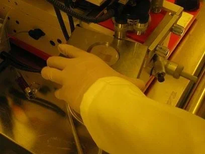 Printed circuits are created using equipment with integrated high-resolution microscopes for the alignment process. UV light is passed through a previously imprinted mask to transfer a pattern to the conductor.Copyright 2015 Wearable Electronics Laboratory, Energy Park Unit, Mechanical Engineering Department, University of Houston
Students are introduced to the technology of flexible circuits, some applications and the photolithography fabrication process. They are challenged to determine if the fabrication process results in a change in the circuit dimensions since, as circuits get smaller and smaller (nano-circuits), this could become very problematic. The lesson prepares students to conduct the associated activity in which they perform statistical analysis (using Excel® and GeoGebra) to determine if the circuit dimension sizes before and after fabrication are in fact statistically different. A PowerPoint® presentation and post-quiz are provided. This lesson and its associated activity are suitable for use during the last six weeks of the AP Statistics course; see the topics and timing note for details.
Wearable electronics, that is, electronics that are highly bendable and conformable, have attracted a great deal of attention and development in the last decade because they enable classes of applications that are impossible to be addressed with wafer-based technologies (for example, Google Smart Lens). Among their great advantages, wearable electronics are relatively large in area, thin, lightweight, mechanically flexible, stretchable and conformable. They can also enable continuous mobile health-monitoring on animal bodies. With wearable electronics, engineers are able to design solutions for challenges such as: What if electronics were soft and pliable? What if electronics conformed to us, instead of us conforming to electronics? Within this context, students see a real-world applied use for statistical analysis.
Photolithography is the process used to fabricate flexible wearable electronics—a process that resembles the film photographic process used years ago. A very thin conductor foil is adhered on a glass substrate coated with a thin layer of polyimide; then the conductor is covered with a layer of photoresist (a photo-sensitive polymer). Upon exposing to UV light through a mask containing various patterns, chemical reactions happen on the light-exposed regions. The exposed photoresist is selectively washed away with a chemical solution and the conductor foil is exposed for further processing. Because of light diffraction phenomena in the photoresist coating, errors occur in the pattern transfer process, producing changes in the circuit dimensions that might affect the strain and stress properties (such as conductivity and resistivity) of conductors. While no evidence exists that these changes in circuit dimensions affect the reliability or performance of the circuits, determining if these changes are the same for any circuit or if the changes depend on the original circuit size, has the potential to be used as part of a procedure to determine what could be the smallest reliable circuit produced via photolithography.
Due to the complexity of mathematically computing the change in dimensions due to diffraction, students use an empirical method in the associated activity. Using the free GeoGebra application, students determine dimension changes in printed circuits, comparing measurements on circuit images taken before and after the manufacturing process. The data obtained is exported to Excel® for analysis. A statistical test for the circuit width differences is performed to verify whether the changes during the fabrication process are statistically significant. Relative dimensions changes are estimated for different circuits, and a correlation between the circuits' relative dimension change and circuits' original size, is obtained.
After this lesson, students should be able to:
- Explain all steps of the photolithography process in the correct order.
- Use technology and a scale factor to obtain indirect measurements of physical objects using images of them.
- Create a procedure to collect, clean and prepare data for hypothesis testing using students' T-distributions.
- Apply logarithmic-exponential functions, and linear correlation analysis to find relationships between experimental data.
- CCSS.Math.Content.HSS-IC.B.5 Use data from a randomized experiment to compare two treatments; use simulations to decide if differences between parameters are significant.
Grades 9-12
Do you agree with this alignment?
- Medical technologies include prevention and rehabilitation, vaccines and pharmaceuticals, medical and surgical procedures, genetic engineering, and the systems within which health is protected and maintained.
Grades 9-12
Do you agree with this alignment? - STEL-8Q Synthesize data and analyze trends to make decisions about technological products, systems, or processes.
Grades 9-12
Do you agree with this alignment?
- HS-ETS1-1 Analyze a major global challenge to specify qualitative and quantitative criteria and constraints for solutions that account for societal needs and wants.
Grades 9-12
This resource focuses on the following Three Dimensional Learning aspects of NGSS:
Science & Engineering Practices- Analyze complex real-world problems by specifying criteria and constraints for successful solutions.Do you agree with this alignment?
Disciplinary Core Ideas- Criteria and constraints also include satisfying any requirements set by society, such as taking issues of risk mitigation into account, and they should be quantified to the extent possible and stated in such a way that one can tell if a given design meets them.Do you agree with this alignment?
- Humanity faces major global challenges today, such as the need for supplies of clean water and food or for energy sources that minimize pollution, which can be addressed through engineering. These global challenges also may have manifestations in local communities.Do you agree with this alignment?
Crosscutting Concepts- New technologies can have deep impacts on society and the environment, including some that were not anticipated. Analysis of costs and benefits is a critical aspect of decisions about technology.Do you agree with this alignment?
Do you agree with this alignment? - Analyze complex real-world problems by specifying criteria and constraints for successful solutions.
- AII.9-12.1.B use a problem-solving model that incorporates analyzing given information, formulating a plan or strategy, determining a solution, justifying the solution, and evaluating the problem-solving process and the reasonableness of the solution;
Grades 9-12
Do you agree with this alignment?
- CSI.2.A create and properly display meaningful output;
Grades 9-12
Do you agree with this alignment? - CSI.2.C use Graphical User Interfaces (GUIs) to create interactive interfaces to acquire data from a user and display program results;
Grades 9-12
Do you agree with this alignment?
This end-of-the-year lesson is directed to students taking AP Statistics. Specific required skills are:
- Hypothesis testing for dependent and independent samples
- Experimental design skills to obtain simple random samples
- Linear regression
- Algebra 2/pre-calculus, specifically logarithmic and exponential functions
In addition, basic computer skills in using Microsoft® Excel® and GeoGebra are necessary.
Overview
The purpose of this lesson and its associated activity is to apply hypothesis testing to discover whether the observed changes in circuit dimensions (mainly the circuit widths) during the photolithography process are statistically significant. In other words, if the photolithography process affects the dimensions of the circuits with a certain level of significance, and that these dimension changes are not by chance. This statistical analysis requires students to work with data sets of circuit dimension measurements, one measurement from each original design (mask), and a corresponding measurement from the final printed circuit. Then, from these data sets, students obtain a correlation between the average size change and the average original width of the circuits.
The Photolithography Process
Let's begin by briefly describing the real-world activity context—the photolithography process in nano-circuit fabrication. In very simple terms, photolithography is a process by which images or patterns are transferred to a matrix. Similar to film photography, in which light prints onto sensitive paper an image that was previously printed on a film (negative), photolithography is used to print on a matrix coated with a conductor the image of a circuit that was previously printed on a mask. Since 1935 when Louis Minsk of Eastman Kodak developed the first negative photoresist, photolithography has been used successfully for circuit printing.
But, why and how is this old technique used in modern nanotechnology? Modern nano-circuits are designed using specialized software that is able to test circuits before they are fabricated, that is, the software simulates the functioning of the circuits. Once the circuits work as desired, they are printed on transparent film using specialized high-resolution printers. Then the circuit is fabricated with conductor material. Photolithography an efficient process to transfer the circuit pattern on a mask to a conductor surface. The photolithography process is summarized in the next steps: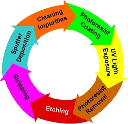 Figure 4. The basic seven steps of the photolithography process, starting with "sputter deposition"—the fabrication of the matrix onto which the circuit will be transferred.Copyright 2015 Wearable Electronics Laboratory, Energy Park Unit, Mechanical Engineering Department, University of Houston
- Sputter deposition: A method of depositing the thin films of a conductor material by way of eroding a target source onto a non-conductor substrate. This is typically accomplished by bombarding the target (source of deposition material) with inert gas atoms. Atoms on the target fly to the substrate.
- Cleaning impurities: Organic/inorganic contaminations are usually removed by wet chemical treatment using solutions containing hydrogen peroxide. Alternatively, sometimes solutions made with trichloro-ethylene, acetone or methanol are used.
- Photoresist coating: A wafer coated with a thin conductor is covered with UV light-sensitive liquid by spin coating. This viscous liquid solution is dispensed onto a rapidly spun wafer to produce a uniformly thick layer.
- UV light exposure: Ultraviolet light passes through a mask (a print of the circuit to be transferred to the wafer) placed on the conductor-coated wafer. Light causes a chemical change on the photoresist portions not covered by the mask.
- Photoresist removal: The photoresist that chemically reacted is removed from the substrate. This is usually accomplished by using a liquid resist stripper or developer to chemically alter the photoresist so that it no longer adheres to the substrate.
- Etching: Using a liquid ("wet") or plasma ("dry") chemical agent, the uppermost layer of the conductor substrate is removed in the areas that are not protected by the photoresist.
- Stripping: A solvent called a stripper is used to fully remove the photoresist and any of its residues.
The statistical analysis to be performed in this project requires students to work with data sets of circuit dimensions, one from the original designs (mask) and the other from the final printed circuit. Then, from the data sets obtained from different circuits, students find a correlation between average size change and the circuit's average original width.
Because all the information and parameters necessary for the statistical analysis, mean and standard deviation come from the samples, the hypothesis testing in this problem must be performed using the T-distribution, and two cases can be distinguished: dependent or independent samples.
Dependent samples are like those shown in Figures 5 and 6 (mask) and Figure 7 (printed circuit), in which the corresponding before-and after circuit elements may be identified. Because the same elements on the mask and on the printed circuit pictures are measured, samples will have the same size n. Figure 5. A circuit mask is the equivalent to the negative in the old photographic process, but the dimensions of the elements in this circuit must be measured in μm (micrometers). The elements on this mask are printed on non-conductor material and used to support the circuits.Copyright 2015 Wearable Electronics Laboratory, Energy Park Unit, Mechanical Engineering Department, University of Houston
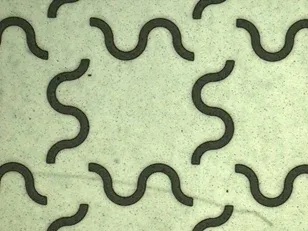 Figure 6. A mask pattern for a network of metallic conductors, connecting nano-components.Copyright 20105 Wearable Electronics Laboratory, Energy Park Unit, Mechanical Engineering Department, University of Houston
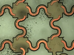 Figure 7. A printed circuit can be created using more than one mask, in this case, one for the dielectric base and another for the metallic conductors, to create a single unit. The corresponding mask elements can be identified in the final circuit.Copyright 2015 Wearable Electronics Laboratory, Energy Park Unit, Mechanical Engineering Department, University of Houston
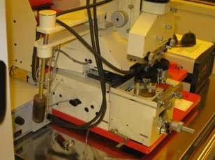 Figure 8. A mask aligner in use at the Wearable Electronics Laboratory in the Mechanical Engineering Department at the University of Houston, TX.Copyright 2015 Wearable Electronics Laboratory, Energy Park Unit, Mechanical Engineering Department, University of Houston
Independent samples can be used in cases in which the corresponding before and after circuit elements cannot be identified. The only requirement is that both samples be of the same kind of circuit elements; samples can be the same or different size.
Both approaches support the same statistical analysis conclusion. To verify this assertion, both analyses are performed in this project. For further analysis, it is useful to know that both methods can support the conclusion and then choose to use the most convenient or easier to implement.
For dependent samples, hypothesis testing is performed on the data differences. An Excel® table of sample data is shown in Figure 9. Data graphs of data differences are shown in Figures 10 and 11.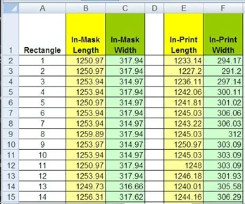 Figure 9. Using the measuring interface, collected data for dependent samples is arranged in a table, identifying the measured element. Collected data can be analyzed using the Excel® statistical functions, and then data differences can be tested and graphed.Copyright 2015 Wearable Electronics Laboratory, Energy Park Unit, Mechanical Engineering Department, University of Houston
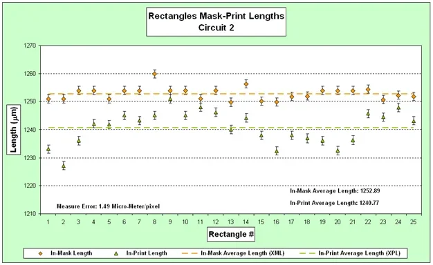 Figure 10. Differences in the average dimensions of mask and printed circuits' corresponding elements (dependent samples) proves that the printing process affects the circuits' dimensions.Copyright 2015 Wearable Electronics Laboratory, Energy Park Unit, Mechanical Engineering Department, University of Houston
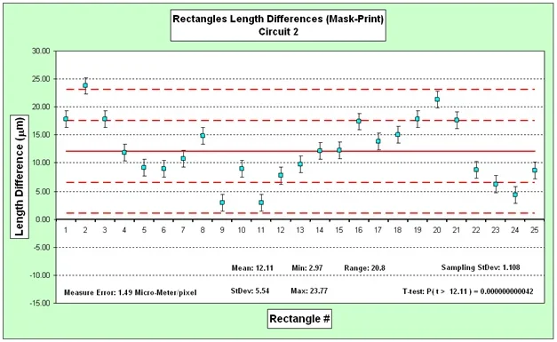 Figure 11. The positive average value of the differences (before and after printing) in the circuits' dimensions, and the low probability to obtain a sample with this mean, indicates that the printing process affects (reduces) the dimensions of the circuits.Copyright 2015 Wearable Electronics Laboratory, Energy Park Unit, Mechanical Engineering Department, University of Houston
The t-statistics corresponding to the average d̅ of these paired differences (Figure 10) is computed using the equation: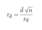
where sđ = standard deviation of the differences, and n = sample size.
Using the Excel® TTEST() statistical function (refer to http://www.excel-easy.com/examples/t-test.html), the P-value (P(t ≥ t đ)) corresponding to this statistic is calculated. Then this P-value is compared with the chosen significance level, usually 0.01 ≤ α ≤ 0.1, concluding the test. If the calculated P-value is less than the significance level, the average difference is statistically different from zero, with a confidence level of 1-α. This result provides evidence that changes in the circuit dimensions occurred in the photolithography process.
For the independent samples test, a random sample of mask parts are compared to a random sample of the same kind of printed circuit parts. The samples may be of different sizes; in this case, graphs like those in Figures 10 and 11 are not possible. Even if the samples are of the same size, the differences in these values cannot be taken because it is not the same set of elements before/after a process. The statistical analysis focuses only on the difference of the samples' means. The corresponding t-statistic is computed using the equation: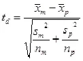
where x m is the average circuit's mean width in-mask, and xp are the average circuit's width after printing; sm and sp the corresponding samples standard deviations, and nm and np the samples sizes.
Using the Excel® TTEST() statistical function, the P-value (P(t ≥ t đ)) corresponding to this statistic is calculated. This P-value is again compared with the chosen significance level (α), and if the P-value is less than the significance level, the means of the two data sets are statistically different, with a confidence level of 1-α. This supports the argument that changes in circuit dimensions occur in the photolithography process.
The next step is to collect data of the relative size changes from different circuits' widths, where this relative change is defined as relative size change (%):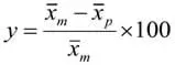
Then graph the relative change y-values versus the original mean widths x̄m. Expect the resulting graph to be similar to Figure 12.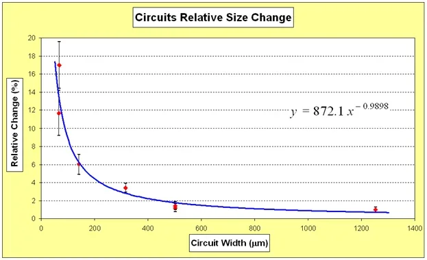 Figure 12. Power regression between circuits' average change and original in-mask circuits' width; the average change is inversely proportional to the circuit's width.Copyright 2015 Wearable Electronics Laboratory, Energy Park Unit, Mechanical Engineering Department, University of Houston
By using the graph built-in option add-trend line (click on one of the data points, then right click), Excel® computes a non-linear correlation function for these points. But given that only linear correlations are in the scope of an AP Statistics course, something must be done on these points to make them fit a linear correlation.
The algebraic trick taught in Algebra 2 and Pre-Calculus is the application of logarithms to the above data. Because these points fit a power correlation, it is well know that logarithms can remove powers, as stated in their power property:
ln(xn )=n∙ln(x)
So, adding to the Excel® data table two extra columns, computing in one of these columns the log of the relative change and in the other the log of the circuit original dimension, then graphing these log entries, these points now exhibit a linear pattern (see Figure 13).
The linear correlation function can be easily determined using the add trend line option again; in this case, we find that the linear correlation is: y = -0.9898 x + 6.7709.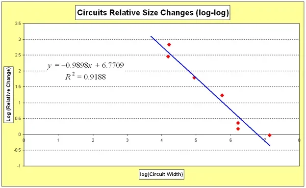 Figure 13. The linear regression achieved in this log-log graph leads to a power correlation between the circuits' average size change and the circuits' original in-mask width.Copyright 2015 Wearable Electronics Laboratory, Energy Park Unit, Mechanical Engineering Department, University of Houston
But this equation is really of the form:
ln(relative change) = -0.9898•ln(circuit width) + 6.7709
Using the log's power property and applying the exponential function to both sides of this equation:
ln(relative change) = ln(circuit width)-0.9898 + 6.7709
exp[ln(relative change)] = exp[ln(circuit width) -0.9898 + 6.7709]
The power relationship in Figure 12 can be obtained:
relative change = 872.1 (circuit width)-0.9898, where 872.1 = e6.7709
This equation can be used to predict changes in printed circuits during the photolithography process, initially valid for the Carl Suss MJB3 mask aligner model.
While the previous paragraphs describe how to perform the appropriate statistical analysis of the data; the next paragraphs explain how the data for this analysis are generated or obtained.
Given that these masks and circuits are very small, measuring requires a high-resolution microscope, an integrated camera and imaging software (see Figures 14 and 15), typically resources only available in universities research labs.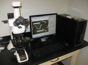 Figure 14. Equipment used at the University of Houston's Wearable Electronics Lab to inspect and measure nano-circuits.Copyright 2015 Wearable Electronics Laboratory, Energy Park Unit, Mechanical Engineering Department, University of Houston
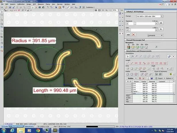 Figure 15. Imaging software used to visualize and measure portions of nano-circuits. The least measurement precision achieved is 2.94 μm/pixel.Copyright 2015 Wearable Electronics Laboratory, Energy Park Unit, Mechanical Engineering Department, University of Houston
For students' practice, picture sets of these circuits (Nano-Circuit Picture Sets zip file (ZIP)) were taken using the Nikon Eclipse LV100ND microscope with attached Lumenera Infinity1 video camera, and NIS-Elements 4.20 imaging software.
To measure the circuits' dimensions on these pictures, use the provided graphic interface developed using the GeoGebra geometry software (Figure 16). Importing circuit and mask images as backgrounds, it is possible to draw on them and determine on-screen distances between points, as well as the dimensions of the drawn geometric shapes.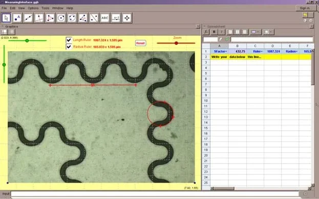 Figure 16. This GeoGebra interface simulates the NIS-Elements imaging software. Measurements made with the integrated rulers can be recorded in the integrated spreadsheet.Copyright 2015 Wearable Electronics Laboratory, Energy Park Unit, Mechanical Engineering Department, University of Houston
The obtained data can be manually recorded in the GeoGebra integrated spreadsheet (see Figure 16). To transform these on-screen measurements to the real circuit's dimensions, an appropriate scale factor must be used, and is already set up in the measuring interface.
Once the information is ready, it can be exported to Excel® in order to perform the corresponding graphing and statistical analysis. Refer to the basic GeoGebra and measuring interface practices in the associated activity attachments.
(Be ready to show students the 17-slide Flexible Circuits: Project Scope Presentation (PPTX), two online articles about the Google Smart Lens and an online link showing some mathematical calculations. Make copies of the Post-Introduction Quiz (PDF), one per student. Note: The slides are "animated," so run the PowerPoint® file as a slide show and click to bring up the next item.)
(Slide 1) The title slide includes a quotation by Peter Macleod about flexible circuits being a high-growth technology of the 21st century.
(Slide 2) What is diabetes? Do you know a person who has diabetes? (Listen to student answers and stories.) What precautions must a diabetic person take in order to avoid complications from high blood sugar levels? (Listen to student answers.)
(Slide 3) Diabetes care includes general medical care, medication, regular exercise and smart lifestyle choices, a good diet and ongoing glucose (blood sugar) monitoring. Many diabetic people, if not all, must poke their fingers once or more times a day in order to measure their blood sugar levels, also called blood glucose levels. Look at this photograph of a typical device used for blood testing. (The device is shown on the slide is similar to Figure 1.) This daily blood testing procedure is an unavoidable routine since monitoring and controlling of blood glucose levels is critical for diabetics' health, yet it can be an annoying and frustrating process.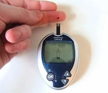 Figure 1. A commercial glucose meter used for blood glucose level testing.Copyright 2007 David-i98, Wikipedia https://en.wikipedia.org/wiki/File:Blood_Glucose_Testing.JPG
(Slide 4) Think about this: We know that sugar levels can be also measured in other corporal (human body) fluids such as sweat and tears. Knowing this, can you think of some alternate solutions to the poking process required for blood testing? (Give students a moment to think about it and then listen to their ideas, writing them on the classroom board.)
(Slide 5) Here's an example idea. (Show the class one or both of the online articles about the Google Smart Lens, accessibly by clicking on the blue buttons on the slide; the website URLs are also provided in the slide notes and the Additional Multimedia Support section.) This alternative approach—called the smart lens—was developed by Google labs and other research laboratories. The lens can measure blood sugar levels directly from tear fluid on the eyeball surface! The lens contains a low-power microchip and a nearly invisible and flexible circuit.
(Slides 6-11) At the core of this invention is the use of flexible electronics. Has anyone heard of flexible electronics? (See if any students know about it. Next, explain the flexible electronics' concept, show applications, and the standard fabrication process: photolithography. Working from the photolithography fabrication process diagram on slide 11, click on each colored arrow to see a brief explanation of each step of the process; this feature is enabled via "custom shows" that automatically return back to slide 11. At this point, if desired, add more content from resources suggested in the Additional Multimedia Support section.)
(Slide 12) The UV-printing step in the photolithography process is the starting point for the core activity of this lesson. (Refer to the simplified UV-printing process diagram on the slide, which is the same as Figure 2. Emphasize that the circuit mask is placed over UV sensitive material [photoresist] and the separation between the mask and the conductor is just the photoresist coat thickness [about 2 μm].)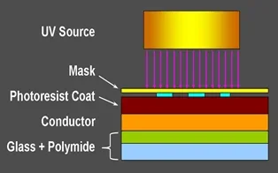 Figure 2. A circuit mask is the equivalent to the negative in the old photographic process. It is placed on UV-sensitive material to cast a shadow, with the expectation that an exact copy of the shape in the mask is printed.Copyright 2015 Miguel R. Ramirez, RET Program, University of Houston
(Introduce the challenge questions.) Do you expect that the printed circuit is an exact copy of the mask? Or is there something in this procedure that may produce changes?
(While displaying Figure 2, emphasize the importance of this question.) This questions is important because, even though at present no evidence exists that changes in circuit dimensions during the fabrication process affect circuit reliability or performance, researchers in this field think that a severe change in circuit dimensions may possibly affect mechanical properties such as strain and stress, or conductivity-resistivity. (Initiate a class discussion with the entire class or in small groups, writing on the classroom board what students think may alter circuit dimensions. Expect students to mention diffraction as a possible cause.)
(Click on slide 12 so Figure 3 appears, which is slightly different than Figure 2.) During the UV-printing step, UV light is diffracted and according to specialists, may be the primary cause in circuit dimension changes. Other steps in the process, such as etching, may also contribute to this change.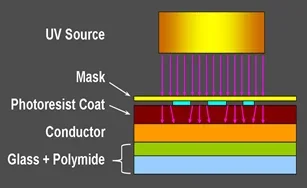 Figure 3. Diffraction occurs when light encounters an obstacle or passes through a narrow slit. Diffraction is more important as the dimensions of the obstacle/slit are comparable to the light wavelength.Copyright 2015 Miguel R. Ramirez, RET Program, University of Houston
How can we know if the photolithography process alters the circuit dimensions or not?
(To guide students to the desired answer, which is to compare printed circuits with their corresponding original designs, show students this link: http://www.mike-willis.com/Tutorial/diffraction.htm so they see that the mathematical solution for diffraction is extremely complex!)
(Once students suggest the comparison solution, address the entire class as follows.) Visualize yourselves as engineers working in the production of nano-circuits. You must determine if your fabrication process alters the original circuit design dimensions or not. You know of no complaints about quality or performance, but every time smaller circuits are demanded, a change in the dimensions may be a more serious problem. How do you suggest we proceed?
(Expect students to answer with the following suggested approach: measure a random sample of original designs and compare these measurements with the measurements of the corresponding printed circuits.)
(Show slides 13-14. At the end of slide 14, ask the class the following questions.) Is it good enough to just compute the differences in the measurements? How can you know if the observed changes are really caused by the photolithography process and not produced only by chance? (Depending on student answers, give them hints that the correct analysis to perform in this case is hypothesis testing.)
(Once students give hypothesis testing of the data as the answer for this question, show slide 15 and pose the next question to the class.) How could you know from the data if the change is the same for any circuit size or if it depends on the original circuit's size? Or alternatively, do a very tiny circuit's dimensions change the same as a circuit that is 10 times bigger, or do the smaller circuit's dimensions change more than the larger circuit's dimensions, or do the larger circuit's dimensions change more than the smaller circuit's dimensions?
(Depending on students' answers, give them hints that the only way to know this is by collecting measurement data from different circuit sizes, and trying some kind of correlation on this data. Show slide 16 to introduce the computation for "relative size.")
(Conclude the session with the following question.) What is the benefit of determining a correlation for the data? (The expected answer is: With such correlation, the specific change for a given circuit's dimension can be predicted, or can be used to calculate dimensions of the circuits on the mask, to produce specific dimensions in the printed circuit. After this question/answer, show slide 17.)
Congratulations! Our next step is to conduct the associated activity Applying Statistics to Nano-Circuit Dimensions in Fabrication during which you will analyze the available data to develop solutions to answer these questions and then present them in a professional way.
(Conclude the lesson by administering the quiz.)
(After students have completed the lesson and its associated activity.) Now that you have some idea of the potential and present applications of flexible electronics, let your imaginations fly and make a list of at least three possible applications. Don't worry if your ideas sound like science fiction! When your grandparents were kids, a device like an iPad sounded like science fiction to them!
- alternate hypothesis
- Denoted as H1, a statement that directly contradicts a null hypothesis by stating that the actual value of a population parameter is less than, greater than or not equal to the value stated in the null hypothesis.
- coefficient of determination
- A measure of how well the regression line represents the data; labeled as r2. If the regression line passes exactly through every point on the scatter plot, it explains all of the variation and r2=1. The further the line is away from the points, the less it is able to explain the variation of the data and the r2 value approaches 0.
- conductivity
- The degree to which a specified material conducts electricity or heat. It is the reciprocal of resistivity.
- correlation coefficient
- A statistical measure of the degree to which changes to the value of one variable predict change to the value of another; labeled as r. In positively correlated variables, the value increases or decreases in tandem. In negatively correlated variables, the value of one increases as the value of the other decreases.
- dependent samples
- A subset of a population whose elements are measured "before and after" a situation. Also called paired or matched samples.
- diffraction
- A deviation in the direction of a wave at the edge of an obstacle in its path. The spreading of waves around obstacles.
- electrical circuit
- A closed loop through which charges can continuously move. A network consisting of a closed loop, giving a return path for the current.
- empirical
- Based on testing, experience or observation.
- fabrication process
- In electronics, a sequence of well-defined procedures to manufacture a circuit. The process begins with the circuit design, continues with the preparation of the raw materials to be used in the process, then all the manufacturing steps, and ends with the final product or circuit.
- flexible circuit
- A pattern of conductive traces bonded on a flexible substrate. A circuit printed on a flexible dielectric substrate.
- hypothesis testing
- A process to evaluate the credibility of a hypothesis about a population; uses sample data to infer truths about the entire population.
- independent samples
- Two or more samples that have no effect on one another.
- interface (computing)
- Something that enables separate and sometimes incompatible elements to coordinate or communicate. In computer science, hardware or software designed to communicate information between hardware devices, between software programs, between devices and programs, or between computer and users.
- least-squares method
- A statistical method used to determine a line of best fit by minimizing the sum of squares created by a mathematical function. A "square" is determined by squaring the distance between a data point and the regression line.
- linear regression
- In statistics, an approach for modeling the relationship or dependence between a scalar dependent or response variable y and one or more explanatory variables denoted x, by fitting a linear equation y = a + bx.
- log-log graph
- A two-dimensional graph of numerical data that uses logarithmic scales on both the horizontal and vertical axes. Also called log-log plot.
- mean
- The average value of the data; used to derive the central tendency of the data. Also called expected value.
- measurement uncertainty
- The doubt that exists about the result of any measurement because of the precision of the measuring instrument. A quantification of the doubt about the measurement result, usually defined as: measurement taken ± half of the smallest measurement scale of the instrument.
- nanotechnology
- A branch of technology that deals with dimensions and tolerances of less than 100 nanometers in size.
- null hypothesis
- Denoted as H0, the initial statement or assumption about a population parameter, such as the population mean, that is assumed to be true.
- photolithography
- The process of transferring a pattern or design on a mask to the surface of a silicon wafer or plate, using light, and light sensitive materials on the wafer or plate.
- power regression
- Taking the explanatory variable x and fitting for the response variable "y" a function of the form: y = a•xb, where a, b are constants. The function is based on the linear regression of x and y, with both axes scaled logarithmically. Also known as log-log regression.
- printed circuit
- An electrical device in which the wiring and certain components consist of a thin coat of electrically conductive material applied in a pattern on an insulating substrate.
- resistivity
- A property that quantifies how strongly a given material opposes the flow of electric current.
- significance level
- A criterion for judging a decision regarding a null hypothesis. The criterion is based on the probability of obtaining a statistic measured in a sample if the value stated in the null hypothesis were true. The criterion or level of significance is typically set at 5%. When the probability of obtaining the sample mean is less than 5%, assuming the null hypothesis H0 is true, then the evidence does not support the null hypothesis, and this is rejected (but not taken as false), and consequently the alternate hypothesis is accepted (but not taken as true).
- simple random sample
- An unbiased representation of a group; a subset of a statistical population in which each member of the subset has an equal probability of being chosen.
- simulation
- In science and engineering, the representation of the behavior or characteristics of a physical system through the use of another system, usually a computer running programs based on a mathematical representation of the physical system.
- standard deviation
- A numerical value used to indicate how widely individuals in a group vary.
- statistical analysis
- The mathematics of the collection, organization and interpretation of numerical data, in accordance with probability theory and the application of methods such as hypothesis testing to them.
- strain
- The relative change in shape or size of an object due to externally applied forces (strain is dimensionless): change in length/original length (dL/L).
- stress
- The force per unit area applied to an object.
- type i error
- The probability of rejecting a null hypothesis that is actually true. The largest probability of committing a type I error is the significance level value.
- type ii error
- The probability of retaining a null hypothesis that is actually false.
- ultraviolet light
- A type of electromagnetic radiation with wavelengths shorter than visible light but longer than x-rays; in the range 0.4 × 10⁻⁶ and 1 × 10⁻⁸ meters.
- wavelength
- The distance between two points of the same phase in consecutive cycles of a wave. The distance between one peak or crest of a wave and the next peak or crest.
Pre-Lesson Assessment
Class Discussion: Using an example many students are aware of—the iPhone 6 deformation/bending issue—guide students to think about the possible real-world advantages of flexible electronics: If the iPhone 6 were flexible, any deformation would not be a problem. With students in small groups, show them a 1:29-minute video clip titled, iPhone 6 BENDING Controversy | What's Trending Now at https://www.youtube.com/watch?v=LoZPggszTZQ. Ask: Do you think electronic devices like the iPhone 6 can bend without damage? Have students write down their ideas on how this could be possible —or impossible—if that's what they think. Then lead a brief class discussion during which students share their ideas. Conclude by informing students that current applications of flexible circuits are wide-ranging in a variety of fields. They have evolved to provide durability and reliability in products such as cell phones, TVs, antennas and laptops, as well as hearing aids, calculators, cameras, printers and satellites.
Post-Introduction Assessment
Quiz: After presenting the Introduction/Motivation and slide presentation content to the class, administer the Post-Introduction Quiz (PDF) to verify that students are able to identify the photolithography process steps and their correct order.
Lesson Summary Assessment
Class Discussion: At lesson end, make sure that every student understands why hypothesis testing is the best procedure to evaluate two mutually exclusive statements about a population and determine which statement is best supported by the sample data. To do this, initiate a class discussion using the following question:
- Suppose you have circuit dimension data before and after fabrication. Without a statistical analysis, how could you support or justify the assumption that the fabrication process affects these dimensions?
Expect some students to argue that if the computed averages from both random samples are different, that is a good indicator that the dimensions have changed. To refute this argument, remind them that this conclusion is correct only if the averages are coming from the entire population. Because of sampling error, even for big samples, it is possible to obtain random samples of before and after measurements with different means, even if both of the populations' means were equal.
Guide the discussion to the conclusion that hypothesis testing is the appropriate tool to quantify how likely it is for differences to exist in the computed means, assuming no dimension changes exist because of the fabrication process. A very low probability is evidence against the proposed hypothesis, and a strong indicator that the opposite is happening, that is, the fabrication process changes circuits' dimensions.
During the slide presentation, show students one or both of the following articles about the Google Smart Lens: Google Smart Contact Lens Focuses on Healthcare Billions at http://www.forbes.com/sites/leoking/2014/07/15/google-smart-contact-lens-focuses-on-healthcare-billions/ and Novartis Licenses Google's Smart Lens Technology at http://hexus.net/mobile/news/accessories/72117-novartis-licenses-googles-smart-lens-technology/.
More detailed and visual descriptions of the photolithography steps may be found in the online tutorials for this project at https://www.sophia.org/playlists/ap-statistics-second-semester-project.
For a simple and clear explanation of diffraction, watch Daniel Marble's Wave Diffraction video (6:51-minutes) at: https://www.youtube.com/watch?v=o5k_DvHDYq4
GeoGebra channel at YouTube: https://www.youtube.com/user/GeoGebraChannel
GeoGebra website at http://www.geogebra.org/cms/en/
For free tutorials and materials related to this lesson/activity set, see Sophia at http://www.sophia.org/; requires students to set up user accounts; tutorial topics include Excel® statistical functions and graphing data, GeoGebra basics, photolithography, wearable electronics, nanotechnology, statistics (hypothesis testing and linear correlation), and logarithmic and exponential functions.
Bell, Stephanie. A Beginner's Guide to Uncertainty of Measurement. Published August 1999. Measurement Good Practice Guide No. 11, Issue 2, National Physical Laboratory, Teddington, Middlesex, UK, 2001. Accessed July 2014. (41-page PDF) https://www.wmo.int/pages/prog/gcos/documents/gruanmanuals/UK_NPL/mgpg11.pdf
Benson, Harris. University Physics. San Francisco, CA: John Wiley & Sons, 1995.
Brase-Brase. Understandable Statistics 8th Edition, Boston, MA: Houghton Mifflin, 2006.
Flexible circuit. Last updated June 1, 2015. Wikipedia, The Free Encyclopedia. Accessed December 10, 2015. https://en.wikipedia.org/wiki/Flexible_circuit
GeoGebra freeware geometry software. Last updated spring 2014. International GeoGebra Institute. Accessed June 22, 2014. (a graphic calculator for geometry, algebra, calculus, statistics and 3D math) http://www.geogebra.org/cms/en/
Hiemenz, Paul C. and Timothy P. Lodge. Polymer Chemistry. 2nd Edition, Boca Raton, FL: CRC Press, Taylor & Francis Group, 2007.
How to Find the Power of a Statistical Test. Last updated January 2014. Stat Trek (Teach yourself statistics). Accessed July 1, 2014. http://stattrek.com/hypothesis-test/statistical-power.aspx
Klein, Stacy S. and Alene H. Harris. (2007) "A User's Guide to the Legacy Cycle." Journal of Education and Human Development. Volume 1, Issue 1, ISSN 1934-7200. Accessed July 2014. http://www.scientificjournals.org/journals2007/articles/1088.pdf
Macleod, Peter. (June 2002) A Review of Flexible Circuit Technology and Its Applications. Prime Faraday Technology Watch, PRIME Faraday Partnership, Pera Knowledge, Wolfson School of Mechanical and Manufacturing Engineering, Loughborough University, Loughborough, Leics, UK. ISBN1-84402-023-1. Accessed July 2014. http://www.lboro.ac.uk/microsites/mechman/research/ipm-ktn/pdf/Technology_review/flexible-circuit-technology-and-its-applications.pdf
Photography. Wikipedia, The Free Encyclopedia. Accessed July 2014. https://en.wikipedia.org/wiki/Photography
Photolithography. Wikipedia, The Free Encyclopedia. Accessed July 2014. https://en.wikipedia.org/wiki/Photolithography
Photolithography. Last modified May 18, 2007. Old NanoLab Page, PowerPoint® Presentations, NanoLab, Department of Physics and Astronomy, University of Oklahoma. Accessed July 2014. (A 15-slide PowerPoint® file about the motivation, history, methods and theories of photolithography) www.nhn.ou.edu/~bumm/NanoLab/ppt/Photolithography.ppt
Willis, Mike. Propagation Tutorial. Last updated December 26, 2006. Propagation via Diffraction. Accessed June 24, 2014. http://www.mike-willis.com/Tutorial/diffraction.htm
Young, Angela. Photolithography – A History and Its Process. Posted November 15, 2011. Alternative Photography. Accessed July 2014. http://www.alternativephotography.com/wp/processes/photolithography/photolithography-a-history-and-its-process
- Statistical Analysis of Flexible Circuits
AP Statistics topics and timing note: This lesson and its associated activity are intended to be taught during the last six weeks of the school year to address some of the last topics covered in the AP Statistics course: hypothesis testing and linear correlation. The time span recommended for this lesson AND its associated activity is three weeks (second semester, last three weeks); if students are unfamiliar with GeoGebra or Excel®, provide additional class periods to complete the associated activity. Use the grades that students obtain in the associated activity as their six-week test grades and the project results presentations as their final test grades.
Contributors
Miguel R. Ramirez; Cunjiang Yu; Minwei Xu; Song Chen
Supporting Program
National Science Foundation GK-12 and Research Experience for Teachers (RET) Programs, University of Houston
Acknowledgements
This digital library content was developed by the University of Houston's College of Engineering under National Science Foundation GK-12 grant number DGE-0840889. However, these contents do not necessarily represent the policies of the NSF and you should not assume endorsement by the federal government.
The authors also thank RET program director Fritz Claydon, RET academic advisors Stuart Long and Debora Rodrigues, RET advisors Mila Taylor and Marjorie Hernandez, as well as the National Science Foundation for its funding of the RET program.
Special thanks to the Wearable Electronics Laboratory (Flexible/Stretchable Electronics) of the Mechanical Engineering Department at the University of Houston's Cullen College of Engineering, and the Lithography Lab in the Texas Center for Superconductivity at the University of Houston Applied Research Hub in the Energy Research Park.
Copyright
2015 by Regents of the University of Colorado; original © 2015 University of Houston